PCBA refers to the process of mounting, plugging in and soldering components on a bare PCB. The production process of PCBA needs to go through a series of processes to complete the production. The editor will introduce the various processes of PCBA production below.
The PCBA production can be divided into several major processes, SMT patch processing → DIP plug-in processing → PCBA testing → finished product assembly.
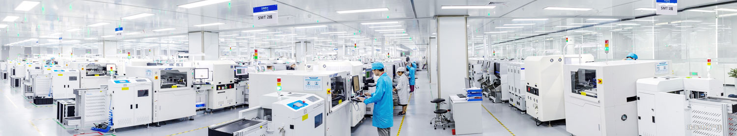
I. SMT patch processing
The process of SMT patch processing: solder paste mixing → solder paste printing → SPI → mounting → reflow soldering → AOI→ rework
1. Solder paste mixing
After taking the solder paste out of the refrigerator and thawing it, stir it by hand or machine to make it suitable for printing and soldering.
2. Solder paste printing
Place the solder paste on the stencil, and print the solder paste onto the PCB pad through the scraper.
3. SPI
SPI is the solder paste thickness detector, which can detect the solder paste printing and control the printing effect of the solder paste.
4. Mounting
Place the SMD components on the feeder, and the SMT head accurately mounts the components on the feeder to the PCB pads through identification.
5. Reflow soldering
Put the mounted PCB board through reflow soldering, the creamy solder paste is heated and turned into liquid through the high temperature inside, and finally cooled and solidified to complete the soldering.
6. AOI
AOI is automatic optical inspection, which can detect the welding effect of PCB board through scanning, and can detect the defect of the board.
7. Rework
Repair the defects detected by AOI or manual inspection.
II. DIP plug-in processing
The process of DIP plug-in processing is: plug-in → wave soldering → cut pins → post-welding processing → board washing → quality inspection
1. Plug-in
Process the pins of the plug-in materials and insert them on the PCB board
2. Wave soldering
Put the inserted board through wave soldering. During this process, liquid tin will be sprayed onto the PCB, and finally cooled to complete the soldering.
3. Cut pins
The pins of the soldered board need to be cut if too long.
4. Post-welding processing
Use a soldering iron to manually solder the components.
5. Washing board
After wave soldering, the board will be dirty, and it needs to be cleaned with board washing water and tank, or by machine.
6. Quality inspection
Check the PCB board, repair nonconforming products, and put conforming products to the next process.
III. PCBA test
PCBA test can be divided into ICT test, FCT test, aging test, vibration test, etc.
The PCBA test is a major test. Different test methods are used according to products and customer requirements.The ICT test is to check the welding condition of components and the on-off condition of the circuit, while the FCT test is to check whether the input and output parameters of the PCBA board meet the requirements.
IV. Finished product assembly
Assemble the passed PCBA boards to the shell, then test, and finally deliver.
PCBA production is linked together, and any problem in any link will have a great impact on the overall quality, so each process needs to be strictly controlled.